Printed Wiring Boards-Design to Prototype
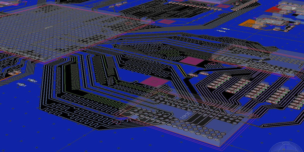
We are able to design printed wiring boards while considering their final expected mass productivity and component mountability.
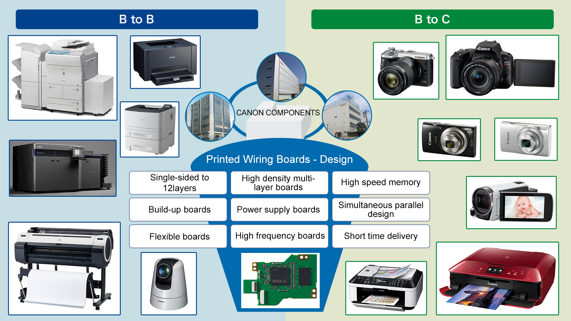
Printed Wiring Boards - Design (Achievements)
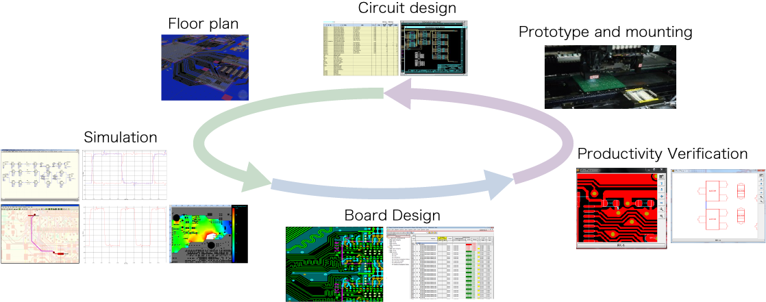
Specification Study to Operation Verification
We support the production of jigs used for evaluation, examination and debugging, starting from the stage of circuit design.
Part survey and selection
Board production, part procurement and part mounting
- Specification study
- Customer's requests will be examined and sophisticated to implementable specifications.
- Part survey and selection
- Selection is made considering the durability and availability of parts.
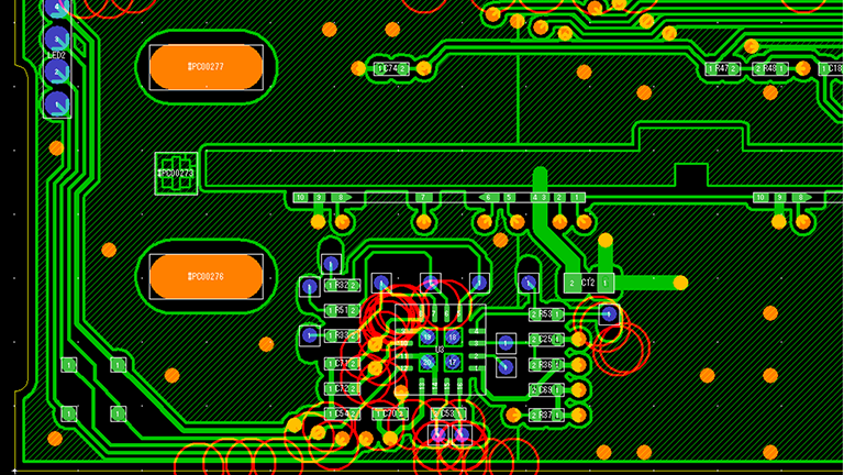
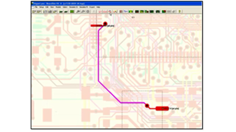
- Circuit design/ Wiring design/ Simulation
- Design work is proceeded collaboratively.
Circuit design (MeBP, DG, OrCAD)/Pattern design (BD, DF, Allegro)/Simulation (signal quality, power quality)
- Board production, part procurement and part mounting
- In cooperation with external manufacturers, board manufacturing and component mounting are conducted.
- Operation verification
- Verification of an open and short circuit, voltage and aspects is carried out.
Simulation
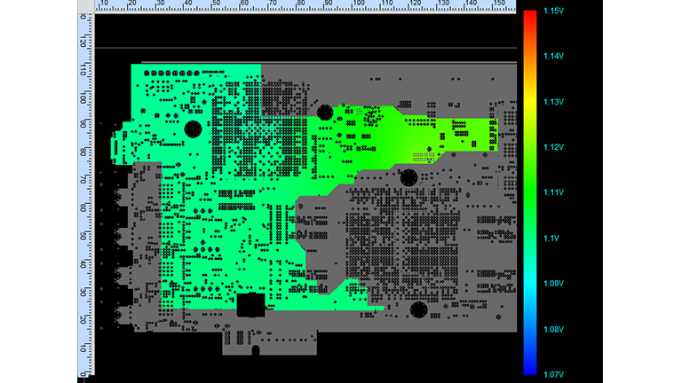
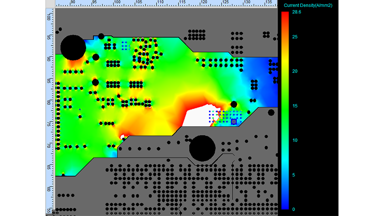
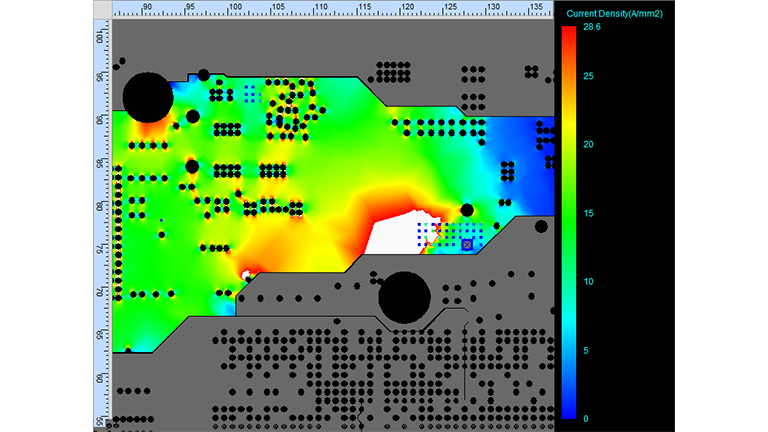
PI (Power Integrity) Simulation
Simulation on power source is performed to feed back the results to design.
- Voltage drop analysis
- Current density analysis
- Impedance analysis
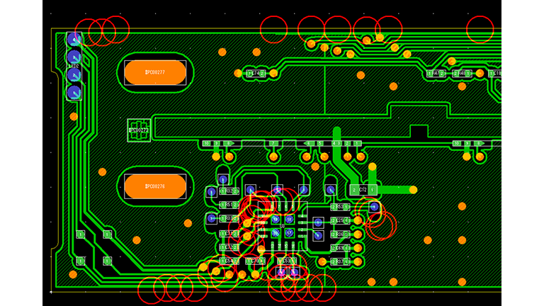
EMI (Electro-Magnetic Interference) Prevention Measures
Boards are designed by taking into account EMI prevention measures.
- EMI check
- Power plane resonance analysis
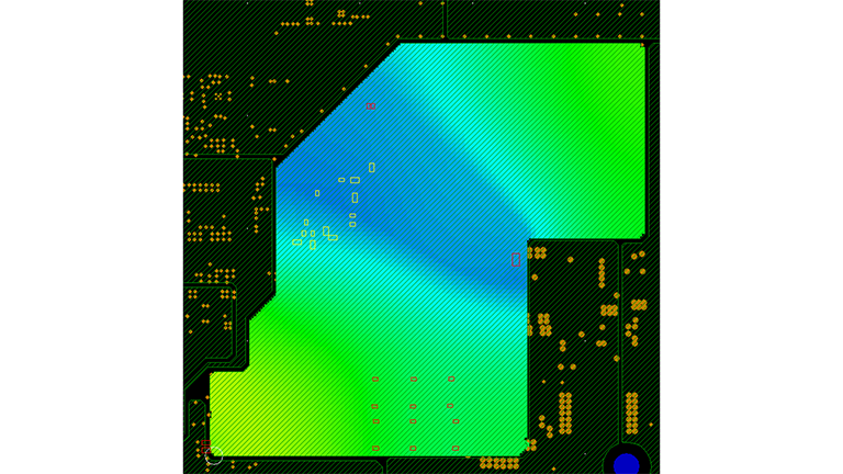
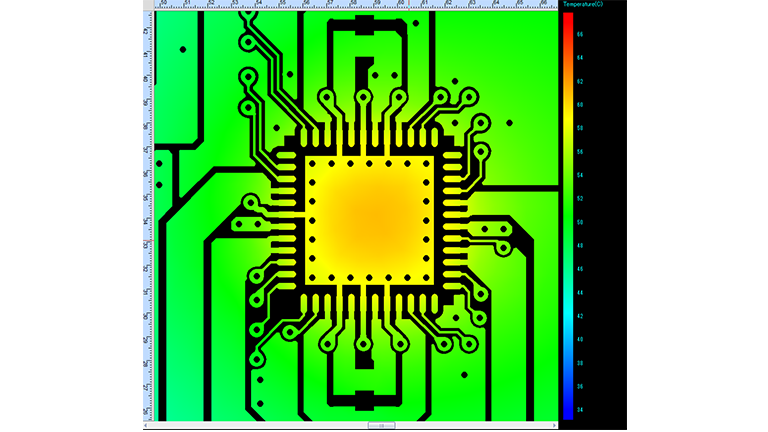
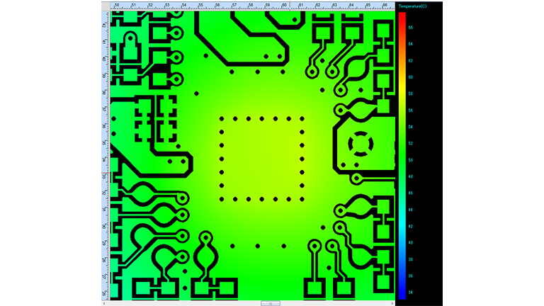
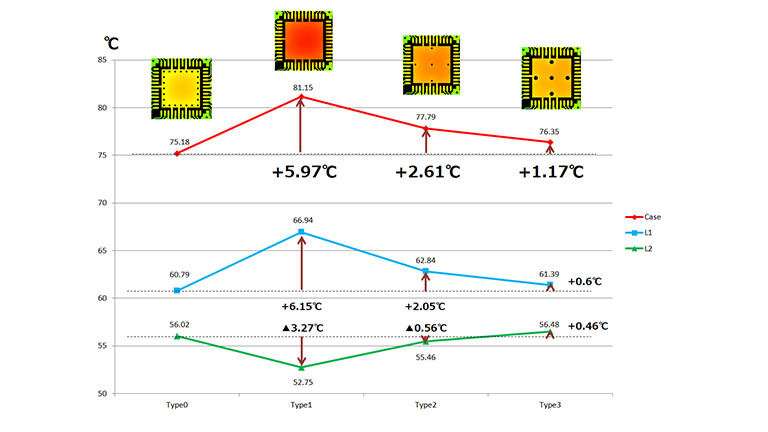
Thermal Analysis
Simulation is conducted in terms of the heat dissipation of a board. We welcome inquiries about simulation content

1.Pre-simulation
please discuss the simulation content with our circuit designer for adjustment
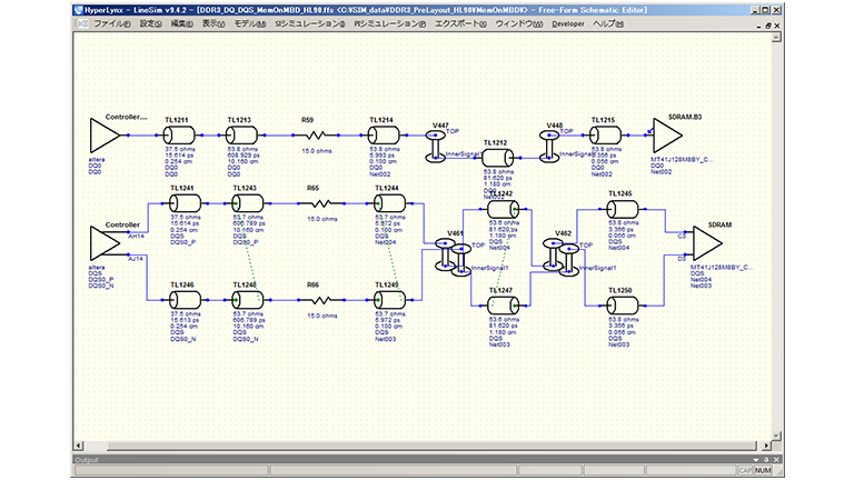
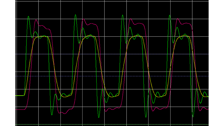
- SI Simulation
- Waveform check/ Damping and termination resistance check/ ASIC buffer capacity check
- PI Simulation
- Voltage drop preliminary check
2.Board Design
- EMI Prevention Measures
- EMI digital check/Power plane resonance analysis
3.Post-simulation
please discuss the simulation content with our circuit designer for adjustment
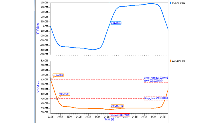
- SI Simulation
- Waveform check/DDR timing margin check
- PI Simulation
- Voltage drop preliminary check/Current density check/Input impedance check
Prototype Boards and Mounting
Development of Libraries, Standards, Verification Tools and Infrastructure
PCB prototype units with high quality will be manufactured at low costs and short delivery times by means of mass production.

Prototype Boards and Production Lead Time
| Through-hole boards |
| Single-sided board |
4days |
| Double-sided board |
4days |
| 4 layer board |
5days |
| 6 layer board |
5days |
| 8 layer board |
6days |
| 10 layer (or more) board |
Please inquire. |
| Build-up boards |
| 1-2-1 |
8days |
| 1-4-1 |
9days |
| 1-6-1 |
9days |
| 2-2-2 |
9days |
| 2-4-2 |
10days |
| 2-6-2 |
Please inquire. |
Lead Time for Prototype Mounting
Where parts are provided by the client: SMT 5 days
- * The schedule above is also applicable even if BGA is present.
- * Although build-up boards with three substrates or more are also available, please inquire us for details.
- * The information here is for guidance. Some requests may not be met depending on their nature.
Design Tools
| Category |
Maker |
Name of tool |
| Logic design |
Intel |
QuartusⅡ |
| Circuit design |
Zuken, Inc. |
Design Gateway |
| Fujitsu Limited |
MeBP |
| CADENCE |
OrCAD |
| Simulation |
Fujitsu Limited |
SignalAdviser SI |
| CADENCE |
PowerDC |
| NEC |
DEMITASNX |
| Board design |
CADENCE |
Allegro |
| Zuken, Inc. |
Board Designer |
| Zuken, Inc. |
Component Manager |
| Zuken, Inc. |
Design Force |
| Zuken, Inc. |
Components Editor |
| Mounting verification |
Zuken, Inc. |
ADM |
| Zuken, Inc. |
DFM Center |
 日本語
日本語 English
